Semiconductor CDMO Chemical Solutions
Accelerating microelectronics and wafer fabrication with high-purity chemical processing, custom synthesis, and dedicated contract development. Built on decades of precision chemical manufacturing, multi-barrier purification, and India's growing semiconductor ecosystem.
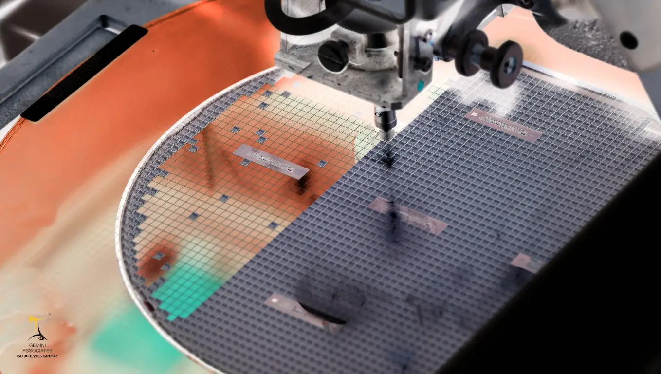
Meeting the Rigorous Demands of Modern Semiconductor Fabrication
Semiconductor manufacturing leaves zero margin for chemical variation. As node geometries shrink and wafer densities surge, contamination control and consistent lot-to-lot purity dictate production yields. Gemini Associates bridges established chemical manufacturing excellence with modern semiconductor CDMO needs.
Extreme Contamination Control
Trace organic residues, metallic particles, and sub-micron particulates can destroy wafer interconnects. Our purification architecture focuses on rigorous multi-stage fractional distillation, filtration, and sealed handling.
Dedicated CDMO Lifecycle
From exploratory route scouting and lab-scale pilot optimization to scaled production, we offer responsive contract development under strict non-disclosure agreements (NDA) and complete customer IP protection.
India Supply Chain Resilience
Aligned with the India Semiconductor Mission (ISM) and global supply chain diversification, our domestic manufacturing and AI-enabled distribution reduce foreign freight dependencies and geopolitical lead-time bottlenecks.
Specialized Chemical Portfolio for Microelectronics
Providing specialized solvent chemistries, surface cleaning formulations, and custom-synthesized chemical building blocks tailored for wafer processing, advanced packaging, and display manufacturing.
Wet Process Cleaning & Surface Solvents
Engineered for wafer surface degreasing, ultrasonic bath cleaning, and critical residue stripping.
Key Chemistries & Formulations:
- Electronic-Grade Anhydrous Ethanol (HARSIL™ ultra-low moisture formulations)
- High-Purity Isopropanol (IPA) for drying and surface solvent dewatering
- Specialty Polar Solvents & Blends for organic particle removal
- De-ionized and ultra-pure water rinse additives
Lithography & Patterning Auxiliary Solvents
High-transmittance solvents and precision intermediates supporting photolithography and wafer patterning.
Key Chemistries & Formulations:
- Edge-Bead Removal (EBR) Solvents with controlled evaporation kinetics
- Photoresist Carrier & Thinner Solvents with tight optical purity
- Developer Auxiliary Rinse Formulations ensuring clean line-edge roughness
- Custom Organic Esters & Ether-Alcohols for specialty resist chemistry
Etching, Stripping & Planarization Intermediates
Specialty chemical building blocks and buffering agents formulated for chemical mechanical planarization and wet etching.
Key Chemistries & Formulations:
- Post-CMP Cleaning Formulations to eliminate slurry particle residue
- Specialty Organic Acids & Chelating Intermediates for controlled etch selectivity
- Precision pH Buffering Systems with lot-to-lot ionic stability
- Surfactants & Wetting Modifiers for high aspect ratio wafer trenches
Bespoke CDMO Synthesis & Contract Formulation
Exclusive contract development and custom manufacturing for proprietary client chemical specifications.
CDMO Capabilities:
- Route Scouting & Laboratory Synthesis of custom electronic intermediates
- Custom Chemical Blending & Recipe Compounding under clean conditions
- Toll Manufacturing & Fractional Purification of client-supplied raw chemistries
- Scale-up from Gram Quantities to Metric Tonnes with full batch validation
Contamination Control Architecture & Analytical Rigor
Every molecule destined for microelectronics must withstand stringent purity scrutiny. Our multi-barrier contamination control and standardized analytical release protocols safeguard chemical integrity from reaction to delivery.
Multi-Barrier Purification
Utilizing fractional packed-column distillation and multi-stage sub-micron cartridge filtration to remove volatile organics, particulate matter, and dissolved contaminants.
Inert Packaging & Barrier Containment
Packed in fluoropolymer-lined, high-density polyethylene (HDPE), and sealed stainless steel containers with nitrogen blanketing to prevent moisture and ambient leaching.
Comprehensive Analytical Profiling
In-house characterization verifying GC/HPLC assay purity, Karl Fischer moisture titration, refractive index, density, non-volatile residue (NVR), and spectroscopic profiles.
Batch Traceability & COA Release
Each production batch is backed by an exhaustive Certificate of Analysis (COA), complete raw material geneaology, and archived retention samples for full regulatory transparency.
The Gemini CDMO Lifecycle: From Concept to Fabrication Release
A structured, milestone-driven partnership framework designed to accelerate your chemical development cycle while maintaining uncompromising quality at every phase.
Technical Feasibility
Review of customer specifications, safety hazard screening, synthetic route scouting, raw material availability, and preliminary cost assessment.
Process Development
Bench-scale synthesis, reaction parameter optimization, impurity profiling, and purification route establishment to maximize yield and purity consistency.
Pilot Synthesis
Gram-to-kilogram demonstration batches, analytical validation, and customer sampling for qualification and fab trial testing.
Scale-Up & Production
Technology transfer to commercial manufacturing modules, rigorous Standard Operating Procedure (SOP) execution, and clean-line packaging.
Quality Release
Final COA validation, QA sign-off, sealed packaging under nitrogen blanketing, and scheduled multi-hub delivery via temperature-monitored logistics.
Transparent Capabilities: Verified Foundation & Future Expansion
Gemini Associates is an established ISO 9001:2015 certified chemical manufacturer operating out of Goa, India, with an aggregate company valuation of ₹2,500M+ and nationwide AI-powered warehousing. Under our active Advanced Materials Expansion initiative, we are investing strategically to scale dedicated clean chemical processing modules, electronic-grade packaging lines, and expanded analytical infrastructure to support India’s semiconductor fab ecosystem.